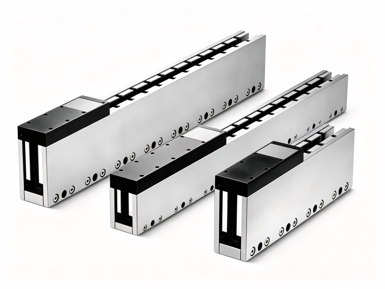
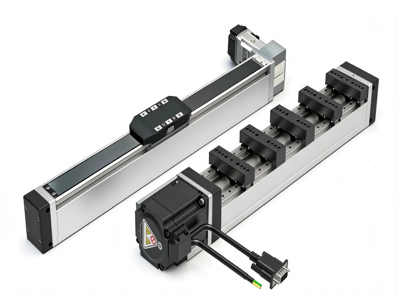
The silicon photonics alignment stage is the single most critical piece of hardware in PIC packaging. Discover why sub-100 nm precision, 6-DOF motion, and active feedback define the future of AI, CPO, and quantum photonics.
The Single Point of Failure in a $3 Billion Industry
Silicon photonics is forecast to become a $3.02 billion test and packaging market by 2034, driven by AI data centers, co-packaged optics (CPO), and quantum computing. But behind every photonic integrated circuit (PIC) — whether it is an 800G transceiver, a LiDAR sensor, or a quantum key distribution chip — there is one piece of equipment that determines whether the device works or fails entirely.
It is not the laser. It is not the DSP. It is the alignment stage.
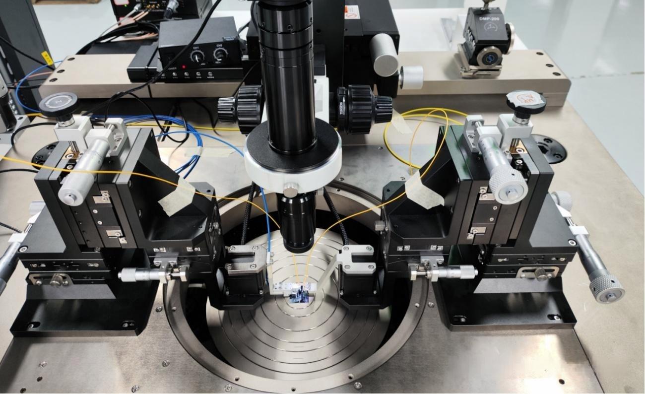
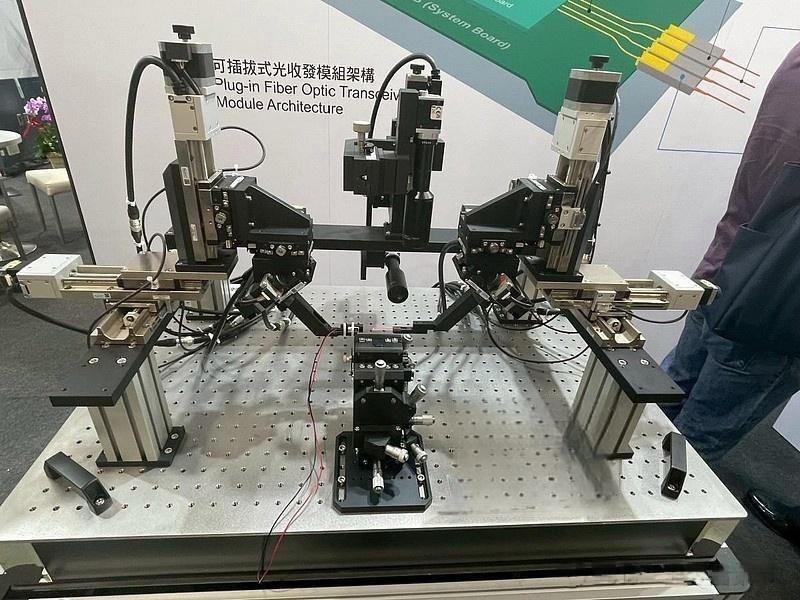
The silicon photonics alignment stage (also called a fiber alignment stage, optical coupling stage, or PIC positioning platform) is the precision motion system that physically brings an optical fiber, lens, or waveguide into contact with a silicon-photonic chip. It is the only piece of hardware in the entire production line that directly controls optical coupling efficiency — and therefore, the only piece that can make or break a device’s performance.
If the alignment stage is off by 50 nanometers, a CPO module loses half its optical power. If it drifts by 1 micrometer during epoxy cure, a $5,000 transceiver becomes scrap. In silicon photonics, the alignment stage is not just a tool. It is the gatekeeper of yield.
What Is a Silicon Photonics Alignment Stage?
A silicon photonics alignment stage is a specialized precision motion platform designed to position optical components relative to a photonic integrated circuit with sub-micron to nanometer accuracy. Unlike general industrial stages, it is engineered specifically for the unique demands of optical coupling:
Multi-axis motion: XYZ translation plus tip, tilt, and sometimes rotation (θx, θy, θz) — up to 6 degrees of freedom (6-DOF).
Sub-100 nm resolution: Required for coupling light into sub-micron silicon waveguides.
Active feedback integration: Real-time optical power monitoring to optimize position before permanent bonding.
Thermal stability: Minimal drift across the -40°C to +85°C operating range.
High-throughput automation: Cycle times measured in seconds, not minutes, for volume production.
The Anatomy of a Silicon Photonics Alignment Stage
Component
Function
Precision Requirement
Linear actuators
Drive X/Y/Z motion
1 nm – 1 µm resolution
Rotation stages
Control tip/tilt for angled coupling
Arc-second level
Encoders
Closed-loop position feedback
0.1 nm – 10 nm
Piezo fine stages
Nanometer-scale trim adjustment
< 1 nm
Controller/software
Gradient search, first-light detection, data logging
ms-level response
Optical power meter
Real-time coupling efficiency feedback
0.01 dB sensitivity
Why the Alignment Stage Is the Critical Bottleneck
Reason 1: It Determines Coupling Efficiency — And Therefore Yield
In silicon photonics, coupling loss is everything. A silicon waveguide has a mode field diameter of roughly 0.3–0.5 µm. A standard single-mode fiber has a mode field diameter of 10 µm. Bridging this mismatch requires either edge couplers or grating couplers — both of which demand sub-micron alignment accuracy.
A 1 µm misalignment can cause 3 dB of coupling loss — half the optical power gone. For an 800G transceiver with 8 parallel lanes, that means 4 lanes worth of signal lost to mechanical error. The alignment stage is the only hardware that prevents this.
Reason 2: CPO Multiplies the Alignment Challenge by 64x
Co-packaged optics (CPO) integrates 16, 32, or even 64 optical channels onto a single switch ASIC. Each channel must be aligned independently — yet simultaneously — because the epoxy cure or laser weld is permanent. A single misaligned channel out of 64 can scrap the entire $20,000+ engine.
This is why6-DOF alignment stageswith multi-channel active feedback have become the critical enabler of CPO manufacturing. Without them, CPO remains a PowerPoint slide, not a product.
Reason 3: Active Alignment Is Impossible Without It
Active alignment — the industry-standard method for high-performance transceivers — works by monitoring optical power in real time while the stage moves the fiber into the optimal position. The algorithm (gradient search, hill-climbing, or machine-learning-based) can only be as good as the stage executing its commands.
If the stage has backlash, the algorithm oscillates. If it has thermal drift, the optimal position shifts during epoxy cure. If it lacks sufficient resolution, the algorithm converges on a local maximum instead of the global optimum. The alignment stage is the physical foundation of every active alignment system.
Reason 4: Wafer-Level Testing Depends on It
Testing PICs at the wafer level — before dicing and packaging — requires aligning optical fiber probes to hundreds or thousands of die sites across a 300 mm wafer. This demands stages with 100 mm+ travel range on at least one axis, yet sub-50 nm repeatability at every stop.
Wafer-level probing is 30% faster than die-level testing and saves an estimated $350 million annually for high-volume fabs. But it is only possible with alignment stages that can maintain nanometer precision across macro-scale travel.
Reason 5: It Is the Most Supply-Constrained Component
While lasers, DSPs, and modulators get the headlines, alignment stages are the silent bottleneck. High-precision piezo and 6-DOF motorized stages are quoting 12–26 weeks delivery in 2026. For a photonics startup closing a Series B milestone or a contract manufacturer racing to qualify for a hyperscaler PO, that delay is fatal.
The alignment stage is not just critical for performance. It is critical for time-to-market.
The Four Types of Silicon Photonics Alignment Stages
Type 1: Manual Alignment Stages
Best for: R&D labs, university research, quick proof-of-concept
Precision: 1–10 µm
Cost: $500 – $3,000
Throughput: 1–2 units per hour
Stock status: Usually available
Manual stages use micrometer heads or differential screws. They are simple, affordable, and require no controllers. But they are far too slow and imprecise for production environments. In silicon photonics, they are primarily used for initial feasibility studies and teaching.
Type 2: Motorized XYZ Alignment Stages
Lead time: 4–8 weeks
Best for: Production lines for 100G/400G transceivers, medium-volume PIC testing
Precision: 0.1–1 µm
Cost: $3,000 – $15,000
Throughput: 50–200 units per hour (with automation)
Motorized stages use stepper or servo motors with linear encoders. They are the workhorse of telecom transceiver manufacturing. With active alignment controllers, they can achieve the ±0.5 µm tolerance required for most pluggable optics. However, they hit a wall at 800G and CPO, where sub-100 nm precision is mandatory.
Type 3: Piezo Nanopositioning Alignment Stages
Best for: Silicon photonics wafer probing, edge coupling, quantum optics
Precision: < 10 nm (down to 0.1 nm)
Cost: $15,000 – $80,000+
Throughput: 100–500 units per hour (with fast algorithms)
Lead time:12–26 weeks (most constrained)
Piezo stages use ceramic actuators that expand under voltage. They offer zero backlash, infinite resolution, and millisecond response times — making them indispensable for sub-50 nm silicon photonics alignment. Long-travel closed-loop piezo nanopositioners ensure high throughput and reliable reproducibility in production environments.
For silicon photonics, piezo is not optional. It is mandatory.
Type 4: 6-DOF Hexapod Alignment Stages
Best for: CPO, multi-channel fiber arrays, complex PIC packaging
Precision: Sub-micron across all 6 axes
Cost: $25,000 – $150,000+
Throughput: 200–500+ units per hour
Lead time: 8–16 weeks
Best for: CPO, multi-channel fiber arrays, complex PIC packaging
Precision: Sub-micron across all 6 axes
Cost: $25,000 – $150,000+
Throughput: 200–500+ units per hour
Application
Required Precision
Stage Type
Why
R\&D / university
±1–10 µm
Manual XYZ
Low cost, maximum flexibility
100G/400G transceiver production
±0.1–0.5 µm
Motorized XYZ + active controller
Sweet spot of speed and precision
800G/1.6T transceiver / CPO
±50 nm
6-DOF hexapod + piezo fine stage
Multi-channel, sub-micron across all axes
Silicon photonics wafer probing
±10–50 nm
Piezo XYZ + long travel
Nanometer precision across wafer-scale travel
Quantum optics / cryogenic
< 10 nm
Cryo-compatible piezo
Thermal compensation, minimal drift
LiDAR / automotive
±0.5 µm
Motorized + vision integration
Robust, high-throughput, cost-sensitive
Main Application Scenarios for Silicon‑Photonics Alignment Hardware
AI‑data‑center CPO optical‑engine packaging: Multi‑channel fiber‑array to PIC alignment for 800G /1.6T co‑packaged optics modules.
Wafer‑level silicon‑photonics probing: On‑wafer PIC optical testing before dicing.
Advanced research: Quantum photonics, satellite optical communication payload prototyping.
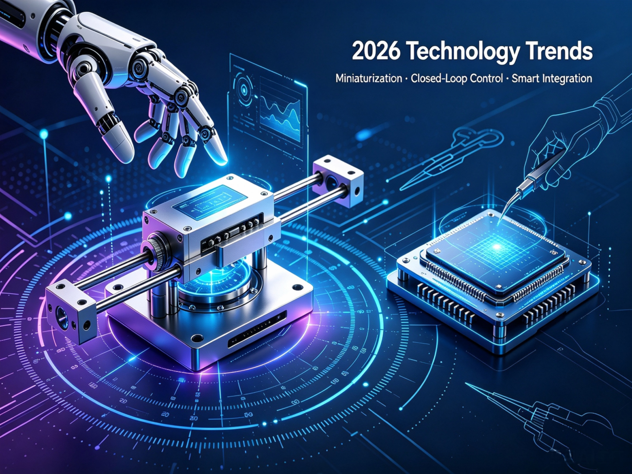
Technical Breakthroughs Redefining Alignment Stages in 2026
1. PILightning: First-Light Detection in Milliseconds
Traditional alignment algorithms spend precious seconds searching for “first light” — the initial optical signal before optimization. PI’s PILightning algorithm solves this problem orders of magnitude faster, reducing total alignment time from minutes to mere seconds.
For high-volume CPO production, this is the difference between 100 UPH and 500 UPH.
2. NxM Simultaneous Multi-Channel Alignment
Conventional systems align one channel at a time. NxM technology aligns any number of inputs (N) and outputs (M) across any number of degrees of freedom (P) — with alignment time virtually independent of channel count. A 64-channel CPO engine aligns in the same time as a single-channel device.
3. Thermal Drift Compensation
Temperature fluctuations cause mechanical drift that degrades alignment. Next-generation stages integrate real-time thermal compensation — monitoring stage temperature and adjusting position commands to maintain sub-50 nm stability across the -40°C to +85°C range.
4. AI-Assisted Gradient Search
Machine-learning algorithms predict optimal alignment trajectories based on device geometry, reducing the number of iterations required for convergence. Early deployments show 18% reduction in false-positive defects and 30% faster wafer release.
5. Modular, Upgradeable Architectures
Instead of replacing entire stages when requirements change, modular designs allow users to swap actuator modules, upgrade controllers, or add axes without scrapping the base platform. This extends equipment life and reduces capital expenditure — critical for startups and R&D labs.
The Supply Crunch: Why Alignment Stage Availability Is the New Spec
In 2026, the photonics industry faces a paradox: demand for silicon photonics devices is exploding, but the alignment stages needed to build them are quoting record lead times.
Stage Type
Typical Lead Time
Market Status
Manual XYZ
1–2 weeks
Available
Motorized XYZ
4–8 weeks
Tightening
Piezo nanopositioner
12–26 weeks
Critical shortage
6-DOF hexapod
8–16 weeks
Supply constrained
The shortage is driven by:
AI data center demand pulling capacity from all precision motion vendors
Shared components (rare-earth magnets, high-precision ball screws) competing with EV and semiconductor industries
Limited qualified suppliers — only a handful of vendors can build stages to silicon photonics tolerances
The implication: In 2026, “In Stock & Ready to Ship” is the most valuable specification for a silicon photonics alignment stage.
How to Evaluate a Silicon Photonics Alignment Stage
The 7-Point Checklist
Resolution vs. repeatability: Resolution tells you the smallest step. Repeatability tells you if it lands in the same place twice. For silicon photonics, repeatability is more important than resolution.
Closed-loop vs. open-loop: Always choose closed-loop with optical encoders. Open-loop stages drift.
Thermal specifications: Verify drift specs across your operating temperature range. A stage rated for 25°C will fail at 80°C.
Software API: Native Python, LabVIEW, and MATLAB support are non-negotiable for modern automation.
Active alignment integration: Does the vendor provide the controller, algorithm, and optical feedback integration — or just the stage?
Service and calibration: Can the vendor calibrate on-site? What is the spare actuator lead time?
Inventory status: Is the stage in stock, or is it a 20-week custom order?
Frequently Asked Questions (FAQ)
What is a silicon photonics alignment stage?
A silicon photonics alignment stage is a precision motion platform that positions optical fibers, lenses, or waveguides relative to photonic integrated circuits (PICs) with sub-micron to nanometer accuracy. It is the critical hardware that determines optical coupling efficiency and therefore device yield.
Why is the alignment stage so critical in silicon photonics?
Silicon waveguides have mode field diameters of 0.3–0.5 µm. A misalignment of just 1 µm can cause 3 dB of coupling loss — half the optical power lost. For CPO modules with 16–64 channels, sub-50 nm alignment is required across all channels simultaneously. The alignment stage is the only piece of equipment that can achieve this.
What is the difference between a motorized and a piezo alignment stage?
Motorized stages use stepper or servo motors and achieve 0.1–1 µm precision. They are ideal for 100G/400G transceiver production.
Piezo stages use ceramic actuators and achieve < 10 nm precision with zero backlash. They are mandatory for silicon photonics edge coupling, wafer probing, and CPO.
What is a 6-DOF alignment stage, and why does CPO need it?
A 6-DOF (six degrees of freedom) stage controls X, Y, Z translation plus pitch, roll, and yaw rotation. CPO modules use multi-channel fiber arrays that must be aligned in all six dimensions simultaneously. Hexapod 6-DOF stages are the only platforms capable of this.
How fast can modern alignment stages align a device?
With advanced algorithms like PILightning and NxM gradient search, alignment times have been reduced to hundreds of milliseconds per channel. Multi-channel CPO engines can be fully aligned in seconds, not minutes.
What should I look for when buying a silicon photonics alignment stage?
Prioritize: (1) repeatability over resolution, (2) closed-loop encoders, (3) thermal stability specs, (4) Python/LabVIEW API, (5) integrated active alignment controller, (6) local service capability, and (7) confirmed inventory / lead time.
Why are alignment stages in short supply?
AI data center demand for 800G/1.6T transceivers and CPO modules has overwhelmed precision motion control suppliers. Piezo and 6-DOF stages share components (rare-earth magnets, precision bearings) with EV and semiconductor industries, creating cross-sector competition. Only a handful of vendors can build to silicon photonics tolerances.
The Alignment Stage Is the Heart of Silicon Photonics
Every photonic integrated circuit — whether it powers an AI data center, a quantum computer, or an autonomous vehicle — must pass through an alignment stage before it becomes a product. It is the point where physics meets manufacturing, where nanometers determine dollars, and where precision becomes profit.
In the $3 billion silicon photonics era, the companies that secure the best alignment stages — with the right precision, speed, and availability — will build the future. The rest will be left waiting for 26-week lead times.
The alignment stage is not a supporting actor. It is the star of the show.
HCY Automation delivers integrated solutions across motion control, linear motion, robotics, machine vision, pneumatic systems, and precision gearboxes to help global manufacturers build smarter, faster, and more reliable production lines. Our engineering team helps you select and integrate the right motion control, robotics, and automation components for your specific application.