High‑precision 6‑axis optical alignment coupling stages for laser diode packaging. Manual‑semi‑auto R&D & fully‑automatic production‑grade multi‑axis positioning platforms for TO, butterfly, COB laser‑diode‑fiber active alignment. Sub‑micron accuracy
What Is a Laser Diode Packaging Precision Stage? (Industry Terminology Guide)
A laser diode packaging precision stage is a specialized multi-axis motion platform engineered specifically for the assembly, alignment, and testing of semiconductor laser diodes. In the photonics manufacturing industry, this equipment is known by several specific terms depending on the context, region, and application:
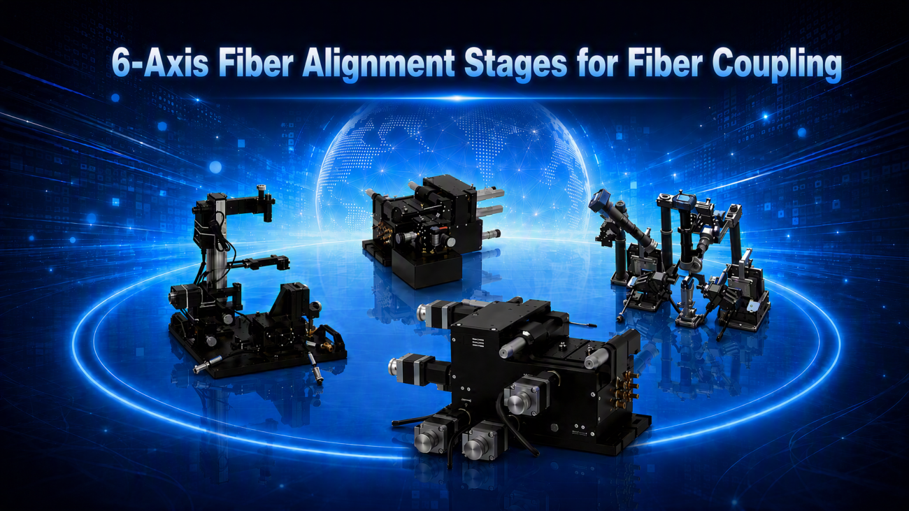
Laser diode packaging demands ultra‑tight positioning accuracy to guarantee stable optical coupling efficiency between laser chips, lenses and optical fibers. The high‑precision motion platforms dedicated to laser diode packaging are widely named optical alignment coupling stages or 6‑axis precision coupling platforms. In mass‑production lines, these core modules are integrated into complete optical alignment coupling packaging systems, serving optoelectronic component assembly from lab prototyping to high‑volume manufacturing.
Optical coupling is the most critical bottleneck in laser diode assembly. Minor positional deviation will drastically reduce light‑transmission efficiency, trigger signal loss and shorten component service life. Therefore, motion platforms must deliver sub‑micron positioning repeatability while supporting multi‑degree‑of‑freedom fine tuning for complex opto‑device structures.
Two Main Application Scenarios: R&D Small‑Batch Prototyping vs Mass Production Packaging
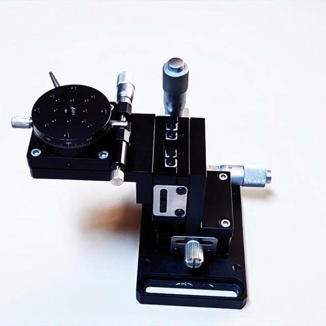
For laboratory research, proof‑of‑concept testing and low‑volume sample preparation, engineers prefer manual or semi‑automatic coupling stages, also known as multi‑axis displacement stages.
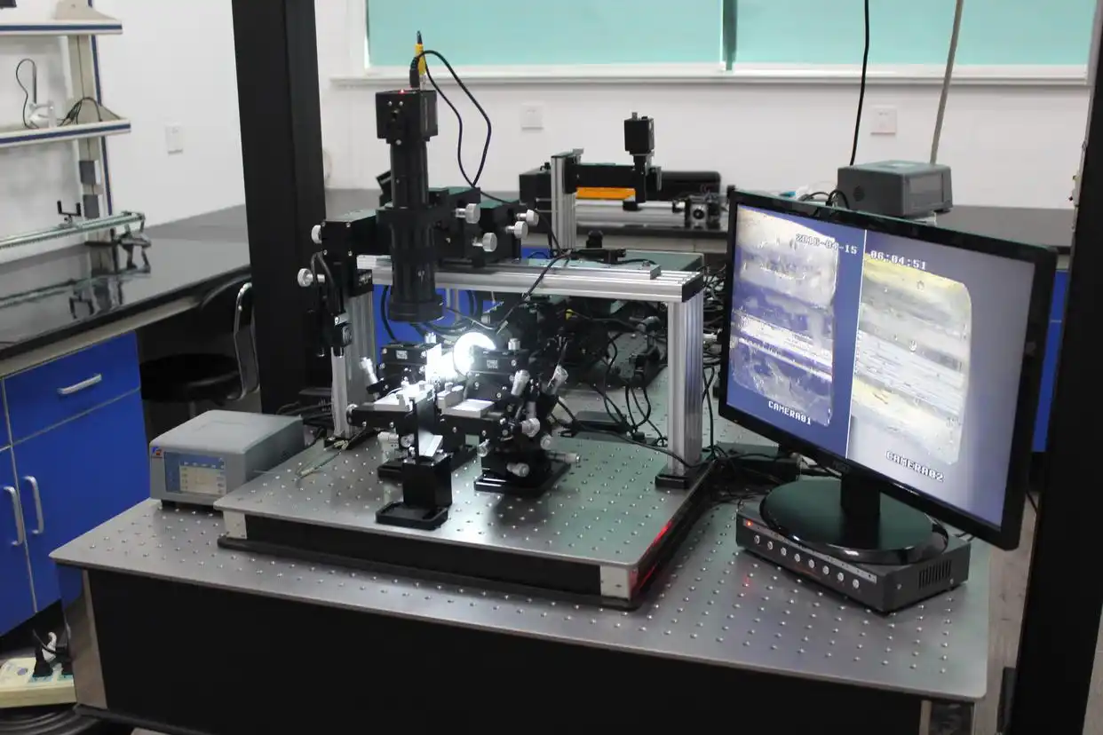
These stages provide full 6‑DOF adjustment: X, Y, Z linear axes plus θx, θy, θz rotational axes. Working together with microscope vision observation systems, they achieve sub‑micron alignment precision (≤0.1 μm). Operators can perform fine iterative positioning to maximize coupling power for TO‑can, butterfly and COB laser diode prototypes.
Typical use‑cases:
New laser diode component prototype validation
Small‑batch trial assembly of custom optoelectronic devices
Lab‑level optical coupling parameter testing
Post‑sample‑production performance verification
Benefits for R&D workflows: flexible configuration, fast setup, low‑cost iteration, no complicated programming for frequent product‑spec switching.
2. High‑Volume Production: Automatic Optical Coupling Packaging System Modules
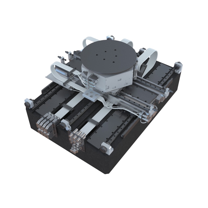
In industrial mass‑production environments, 6‑axis precision coupling platforms work as core functional modules embedded inside fully‑automatic optical coupling packaging equipment.
They execute automatic active alignment and UV curing for mainstream laser‑diode package formats: TO‑can coaxial packages, butterfly‑packaged laser diodes, and COB chip‑on‑board assemblies.
During production cycles, the platform dynamically tracks real‑time optical power feedback. It automatically searches for the optimal spatial position to maximize fiber‑laser coupling efficiency, then locks position and triggers UV adhesive curing. The whole workflow minimizes human intervention, improves yield and shortens cycle time for large‑scale optoelectronic component manufacturing.
A laser diode emits light from an active area typically measuring 1–3 µm in the fast axis and 50–200 µm in the slow axis. Coupling this highly divergent beam into a single-mode fiber (mode field diameter ~9 µm) or a multi-mode fiber (core diameter 50–400 µm) demands sub-micron alignment accuracy.
In butt coupling — the simplest and most common method — the fiber is positioned directly in front of the laser facet. A 1 µm misalignment in the fast axis can drop coupling efficiency by 30–50%. For telecom applications where every decibel matters, this is unacceptable.
Reason 2: Thermal Drift Kills Yield During Epoxy Cure
Laser diodes are temperature-sensitive devices. During packaging, the alignment must be maintained while UV-curable adhesive sets — a process that generates exothermic heat and adhesive shrinkage. Without active tracking (real-time micro-corrections during cure), post-bond shift of even 100 nm can degrade coupling by 0.5–1 dB.
The best optical alignment coupling stages integrate TEC-controlled thermal chucks and active tracking algorithms that monitor optical power throughout the cure cycle, compensating for thermal transients and shrinkage in real time.
High-power laser diode bars contain 10–50 individual emitters on a single chip, each requiring independent fast-axis and slow-axis collimation. Aligning FAC (fast-axis collimation) lenses to these emitters demands 6-axis precision coupling platforms that can handle multiple optical elements simultaneously with sub-micron accuracy across a 10 mm bar length.
Automated FAC alignment stations achieve this in < 25 seconds using 6-DOF platforms with beam analysis feedback.
Reason 4: Butterfly and Coaxial (TO-Type) Packages Require 6-DOF Precision
Coaxial (TO-CAN) packages — the industry standard for low-cost, high-volume laser diodes — require precise fiber-to-chip alignment within a compact cylindrical housing. The optical alignment coupling stage must position the fiber stub with < 1 µm tolerance while maintaining coaxial symmetry.
Pump butterfly laser diodes — the backbone of high-bandwidth optical pumping for data centers and telecom — integrate a laser chip, thermoelectric cooler, thermistor, and precision-aligned optical fiber into a single compact package. The fiber must be aligned to the chip with < 1 µm tolerance while maintaining electrical isolation and thermal contact.
COB (Chip-on-Board) packages — increasingly popular for high-power and multi-channel applications — mount the bare laser chip directly on a PCB or submount. The 6-axis precision coupling platform must align fibers or lenses directly to the chip surface, often with < 50 nm accuracy for single-mode coupling.
This is impossible without 6-DOF optical alignment coupling stages that control X, Y, Z, pitch, roll, and yaw simultaneously, with programmable pivot points that rotate the fiber tip around the laser facet without lateral displacement.
Reason 5: It Is the Most Supply-Constrained Component
While laser diode chips, drivers, and submounts get the headlines, optical alignment coupling stages are the silent bottleneck. High-precision piezo and 6-DOF motorized stages are quoting 12–26 weeks delivery in 2026. For a laser diode packaging house ramping production for an automotive LiDAR design win, that delay can mean losing the program to a competitor with confirmed inventory.
The 4 Types of Laser Diode Packaging Precision Stages
Type 1: Manual / Semi-Automatic Coupling Stage (Multi-Axis Displacement Stage)
Best for: R&D labs, university research, low-volume prototyping
Precision: ≤ 0.1 µm (sub-micron)
Cost: $500 – $3,000
Throughput: 1–2 units per hour
Applications: Initial feasibility studies, wavelength characterization, LIV testing, process development
Configuration: XYZθxθyθz (6-DOF) with micrometer heads or manual differential screws
Key feature: Microscope observation for visual alignment feedback
Manual coupling stages — also called multi-axis displacement stages — use micrometer heads or differential screws for X/Y/Z/θx/θy/θz adjustment. They are simple, affordable, and require no controllers. In R&D environments, they are often paired with high-magnification microscopes for visual observation of the laser facet and fiber position.
They are far too slow for production but essential for process development and die-level characterization before committing to automated production.
Type 2: Motorized Optical Alignment Coupling Stage
Best for: Medium-volume telecom and datacom laser diode packaging
Precision: 0.1–1 µm
Cost: $3,000 – $15,000
Throughput: 20–50 units per hour (with semi-automated workflow)
Configuration: Motorized XYZ + tip/tilt with closed-loop encoders
Motorized optical alignment coupling stages are the workhorse of laser diode packaging. With active alignment controllers, they achieve the ±0.5 µm tolerance required for most telecom and industrial applications. They strike the optimal balance of precision, speed, and cost for medium-volume production of TO-type and butterfly packages.
Type 3: Piezo Nanopositioning Optical Coupling Stage
Best for: High-precision telecom, silicon photonics, quantum optics
Precision: < 10 nm (down to 0.1 nm)
Cost: $15,000 – $80,000+
Throughput: 50–200 units per hour (with fast algorithms)
Configuration: Piezo ceramic actuators with zero backlash
Piezo optical coupling stages use ceramic actuators with zero backlash and infinite resolution. They are indispensable for applications requiring sub-100 nm alignment — such as coupling edge-emitting lasers into single-mode fibers or aligning photonic integrated circuits (PICs) to laser diodes in COB packages.
Type 4: 6-Axis Precision Coupling Platform (6-DOF Hexapod)
Applications: FAC lens alignment, stacked bar assembly, fiber array coupling, beam shaping, TO/Butterfly/COB mass production
Configuration: Parallel-kinematic hexapod with programmable pivot points
6-axis precision coupling platforms — 6-DOF hexapods — use parallel kinematics to control X, Y, Z, pitch, roll, and yaw simultaneously. They enable programmable pivot points — essential for aligning FAC lenses to multi-emitter bars or coupling fiber arrays to high-power pump lasers.
In mass production, these platforms serve as the core motion module inside fully automatic coupling packaging equipment, handling active alignment and固化 for TO-type, butterfly, and COB structures at production speeds.
Typical End‑User Industries
Optical communication component manufacturing (transceivers, laser emitters)
Silicon photonics assembly and testing
Industrial laser diode packaging
Photonics research laboratories & university R&D centers
Medical optoelectronic device assembly
5 Megatrends Driving Demand for Optical Alignment Coupling Stages
1. 800G/1.6T Telecom and Datacom Explosion
Hyperscale data centers are deploying 800G and 1.6T optical transceivers at record pace. Each transceiver requires one or more EML (electro-absorption modulated laser) or DFB (distributed feedback) laser diodes, each of which must be actively aligned to a single-mode fiber with < 0.5 dB insertion loss.
Every EML requires an optical alignment coupling stage for fiber coupling during packaging. The math is simple: more transceivers = more lasers = more alignment stages.
2. Solid-State LiDAR and Automotive ADAS
The automotive industry’s shift toward autonomous vehicles hinges on LiDAR sensing systems, with high-power laser diodes as the core emitters. Solid-state LiDAR modules require 1.5W+ TO emitters embedded into chip-scale units under 10 mm³, with precise focal-axis alignment and long-term reliability.
OEMs are now sourcing directly from packaging houses, bypassing distributors, because they demand tighter control over focal-axis alignment — a process that depends entirely on the 6-axis precision coupling platform.
3. High-Power Industrial and Medical Lasers
High-power laser diodes above 10 watts are poised for a 12.69% CAGR through 2031, driven by additive manufacturing, materials processing, and medical applications. These diodes require stacked bar assembly — aligning multiple laser bars with FAC and SAC (slow-axis collimation) lenses, then coupling the combined beam into a fiber or free-space delivery system. This demands 6-DOF stages with active beam profiling feedback and laser microwelding capability.
4. Pump Butterfly Lasers for Data Center Optical Links
Pump butterfly laser diodes — integrating a laser chip, TEC, thermistor, and fiber into a hermetic package — are the backbone of high-bandwidth optical pumping for cable TV headends, hyperscale data centers, and long-reach telecom.
Each butterfly package requires precision fiber alignment to the chip facet, with sub-micron tolerance, hermetic sealing, and thermal stability. The optical alignment coupling stage is the only piece of equipment that can achieve this repeatable, high-volume assembly.
5. Miniaturization and Wafer-Level Packaging
The drive toward miniaturization is transforming laser diode packaging from traditional TO-CAN and butterfly formats toward wafer-level packaging techniques that enable mass production and cost efficiencies.
Wafer-level packaging requires optical alignment coupling stages with 100 mm+ travel range on at least one axis for wafer-scale probing, yet sub-50 nm repeatability at every die site. This combination of macro travel and nano precision is only achievable with long-travel piezo nanopositioners or hybrid motorized-piezo 6-DOF systems.
The 6-Step Laser Diode Packaging Workflow
Every laser diode package — from a simple TO-CAN to a complex butterfly module — passes through an optical alignment coupling stage during these six critical steps:
Step 1: Die Bonding and Submount Placement
The laser diode chip is die-bonded to a submount (CuW, AlN, or diamond) using eutectic solder or conductive epoxy. The optical alignment coupling stage positions the chip with ±5 µm accuracy relative to the submount’s thermal and electrical pads.
Step 2: Wire Bonding
Gold wire bonds connect the chip’s anode and cathode to the package leads. While wire bonders handle this step, the submount must be precisely positioned on the stage to ensure bond pad accessibility and loop consistency.
Step 3: Optical Alignment — The Critical Stage
This is where the optical alignment coupling stage earns its keep:
For fiber-coupled devices (TO, Butterfly, COB): The stage positions the fiber stub or fiber array in front of the laser facet. Active alignment monitors output power and optimizes X, Y, Z, and angular position to maximize coupling efficiency.
For collimated devices: The stage positions FAC and SAC lenses relative to the chip, using beam profiling cameras to optimize collimation quality.
For multi-emitter bars: The stage aligns FAC lenses to each emitter independently, or uses a single lens bar aligned across the entire array.
Typical performance: Sub-micron accuracy; coupling efficiency > 80% for single-mode; < 25 seconds for FAC lens alignment.
Step 4: Permanent Fixation
Once optimal alignment is achieved, the optical element is permanently fixed:
UV epoxy curing: Low-shrinkage adhesive is dispensed and cured under UV light. Active tracking maintains alignment during cure.
Laser welding: For hermetic packages (butterfly, high-reliability telecom), laser microwelding provides a thermally stable, zero-outgassing bond.
Eutectic soldering: For high-power devices, AuSn solder provides superior thermal conductivity.
Step 5: LIV Testing and Characterization
The packaged device undergoes Light-Current-Voltage (LIV) testing to verify threshold current, slope efficiency, and maximum output power. The optical alignment coupling stage may be used to re-align test fibers or probes for consistent measurement.
Step 6: Final Inspection and Grading
Devices are graded by power, threshold current, wavelength drift, and coupling efficiency. The optical alignment coupling stage ensures that measurement repeatability does not introduce grading errors.
The Technical Battleground: 5 Challenges in 2026
Challenge 1: Fast-Axis Divergence
Laser diodes have extremely high divergence in the fast axis (up to 60° FWHM). Coupling this into a fiber requires either a micro-lens on the chip facet or a separate FAC lens — both of which must be aligned to within ±0.5 µm to achieve acceptable efficiency.
Breakthrough: Automated FAC alignment stations using 6-axis precision coupling platforms with beam analysis feedback achieve sub-micron accuracy in < 25 seconds.
Challenge 2: Thermal Management
High-power laser diodes generate significant heat. Inadequate thermal dissipation can erode efficiency and lifespan, with failure rates climbing to 3% in modules lacking active cooling.
Optical alignment coupling stages must integrate TEC-controlled thermal chucks that maintain the chip at a stable temperature during alignment — typically 25°C ± 0.1°C — to prevent wavelength drift and power fluctuation.
Challenge 3: Post-Bond Shift
Adhesive shrinkage during UV cure can shift the aligned fiber by 100+ nm, degrading coupling efficiency. Active tracking — continuous micro-corrections during cure — is essential to maintain sub-micron alignment.
Breakthrough: Modern optical alignment coupling systems achieve < 50 nm post-bond shift using real-time piezo compensation and low-shrinkage adhesives.
Challenge 4: Multi-Emitter Bar Complexity
A 1 cm laser diode bar contains 20–50 emitters, each requiring independent FAC lens alignment. Traditional sequential alignment is too slow for production. Parallel alignment using multi-lens bars or independent micro-positioners is required.
Breakthrough: Advanced align-attach systems handle multiple element/emitter align-attach with sub-micron accuracy using closed-loop active alignment and beam profiling.
Challenge 5: Cost vs. Precision Trade-Off
Active alignment equipment represents 15–25% of total packaging costs. For price-sensitive markets (consumer electronics, barcode scanning), this is a significant barrier.
Breakthrough: Optimized passive alignment with spot-size converters and V-groove fiber arrays achieves ±2–5 µm tolerance at a fraction of active alignment cost — suitable for multi-mode and lower-power TO-type applications.
How to Choose a Laser Diode Optical Alignment Coupling Stage
The 7-Point Checklist
Package type compatibility: Does the stage support your target package — TO-CAN, butterfly, or COB? Each requires different fixture designs and motion ranges.
Resolution vs. repeatability: For laser diodes, repeatability matters more than raw resolution. A stage with ±50 nm repeatability will produce consistent coupling efficiency across thousands of units.
Closed-loop feedback: Always choose closed-loop with optical encoders. Open-loop stages drift with temperature and load.
Thermal compatibility: Verify TEC integration and temperature stability specs. A stage rated for 25°C ambient will fail at 80°C without active cooling.
Software API: Native Python, LabVIEW, and MATLAB support are non-negotiable for modern automation and AI integration.
Active alignment integration: Does the vendor provide the controller, algorithm, and optical feedback — or just the mechanics?
Post-bond shift compensation: Can the stage perform active tracking during UV cure or laser welding?
Inventory and lead time: Is the stage in stock, or is it a 20-week custom build? In 2026, availability is the ultimate specification.
Frequently Asked Questions (FAQ)
What is a laser diode packaging precision stage?
A laser diode packaging precision stage — also known as an optical alignment coupling stage, 6-axis precision coupling platform, or multi-axis displacement stage — is a multi-axis motion platform that positions optical fibers, lenses, collimators, and submounts relative to a semiconductor laser diode chip with sub-micron to nanometer accuracy. It is the critical equipment that determines optical coupling efficiency, thermal stability, and long-term reliability of the packaged device.
What are the common names for laser diode alignment equipment?
Optical alignment coupling packaging system (when integrated into a production line)
Manual / semi-automatic coupling stage or multi-axis displacement stage (R&D and low-volume)
Core module of fully automatic coupling packaging equipment (mass production)
Why is precision alignment so critical in laser diode packaging?
Laser diodes emit light from an active area measuring 1–3 µm in the fast axis. A 1 µm misalignment can drop coupling efficiency by 30–50%. For telecom applications where every decibel matters, and for high-power applications where thermal management is critical, sub-micron alignment is the difference between a working product and scrap.
What is the difference between active and passive alignment in laser diode packaging?
Passive alignment uses mechanical features (V-grooves, alignment pins) to position fibers without optical feedback. Faster and cheaper, but limited to ±2–5 µm tolerance. Best for multi-mode and lower-power TO-type applications.
Active alignment uses real-time optical power feedback to optimize position before bonding. Achieves sub-50 nm precision and coupling losses below 0.5 dB. Essential for single-mode telecom lasers, EML/DFB devices, butterfly packages, and COB structures.
What types of precision stages are used for laser diode packaging?
Manual / semi-automatic coupling stages (≤ 0.1 µm): R&D and prototyping with microscope observation
6-axis precision coupling platforms / 6-DOF hexapods (sub-micron all axes): Multi-emitter bars, FAC lens alignment, fiber arrays, mass production
What are TO-type, butterfly, and COB packages?
TO-type (coaxial): Cylindrical metal can — highest volume, lowest cost. Used in consumer electronics, PON, and barcode scanning.
Butterfly: Flat hermetic package with TEC and fiber pigtail — used in telecom, datacom, and high-bandwidth optical pumping.
COB (Chip-on-Board): Bare chip mounted directly on PCB — growing for high-power and silicon photonics integration.
How fast can a precision stage align a laser diode?
Manual alignment: 5–15 minutes
Semi-automated active alignment: 30–120 seconds
Fully automated FAC lens alignment:< 25 seconds
Multi-channel fiber array:< 1 second with advanced algorithms
What is post-bond shift, and how do you prevent it?
Post-bond shift is the mechanical displacement of an aligned optical element during adhesive cure or laser welding, caused by thermal transients and adhesive shrinkage. It is prevented by active tracking — real-time piezo micro-corrections that maintain peak coupling efficiency throughout the fixation process.
What are the main applications driving demand for optical alignment coupling stages?
The top 5 drivers are: (1) 800G/1.6T telecom transceivers (39% of laser diode demand), (2) solid-state automotive LiDAR (13% CAGR), (3) high-power industrial lasers (12.69% CAGR for >10W modules), (4) medical and surgical lasers, and (5) pump butterfly lasers for data center optical links.
How much does a laser diode optical alignment coupling stage cost?
Why are optical alignment coupling stages in short supply?
The $9.37B laser diode market is growing at 9.09% CAGR, while precision stage suppliers face shared component competition (rare-earth magnets, precision bearings) from EV and semiconductor industries. High-end piezo and 6-DOF stages are quoting 12–26 weeks delivery. Suppliers with confirmed inventory have a decisive advantage.
The Optical Alignment Coupling Stage Is the Gatekeeper of the Laser Diode Era
Every laser diode — whether it sends data across an ocean, maps the road for an autonomous vehicle, or cuts tissue in an operating room — must pass through an optical alignment coupling stage before it becomes a product. It is the point where physics meets manufacturing, where nanometers determine dollars, and where precision becomes profit.
In the $14.5 billion laser diode era, the companies that secure the best optical alignment coupling stages — whether called a 6-axis precision coupling platform, a multi-axis displacement stage, or the core module of a fully automatic coupling packaging system — will build the future. The rest will be left waiting for 26-week lead times while their competitors ship.
The optical alignment coupling stage is not a supporting actor. It is the star of laser diode packaging.
Conclusion
Whether you need flexible manual/semi‑automatic 6‑axis coupling displacement stages for R&D small‑batch trials, or high‑performance modules for integration into fully‑automatic laser‑diode optical coupling packaging systems, optical alignment coupling stages define the final coupling efficiency and product yield. Selecting the right precision motion platform matching your throughput requirement (R&D prototyping or high‑volume mass‑production) is critical for laser‑diode packaging success.
Are you looking for configurable 6‑axis optical alignment coupling stage solutions for your laser‑diode packaging project? Contact us for technical parameters and application‑matching suggestions.
HCY Automation delivers integrated solutions across motion control, linear motion, robotics, machine vision, pneumatic systems, and precision gearboxes to help global manufacturers build smarter, faster, and more reliable production lines. Our engineering team helps you select and integrate the right motion control, robotics, and automation components for your specific application.